ISLC 2026 Field Notes: Where the PCSEL Actually Stands
The frontier, the boundary, the manufacturing route, and the market
These are first-hand observations from ISLC 2026 (Tampere) on where the PCSEL (photonic-crystal surface-emitting laser) stands: its research frontier and its commercialization routes. Read along four axes (Frontier, Boundary, Route, Market), the picture is of a device class crossing from physical feasibility into engineering and supply-chain execution.
Frontier: How Brightness Scales with Area
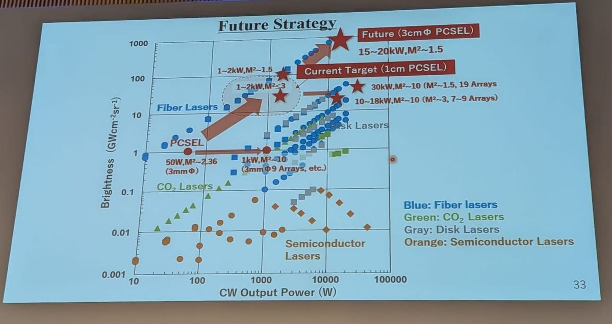
Research group: Prof. Susumu Noda's group, Kyoto University
A laser's value often lies not in raw watts but in brightness (radiance, W·cm⁻²·sr⁻¹): power concentrated into a small spot and a narrow cone. Brightness scales as B ∝ P/(M²λ)², with M² the beam-quality factor and λ the wavelength, so raising it means enlarging the emitting area while holding the beam single-mode. That is the decades-old wall: widen an ordinary laser's aperture and it goes multimode, beam quality collapses, and brightness saturates.
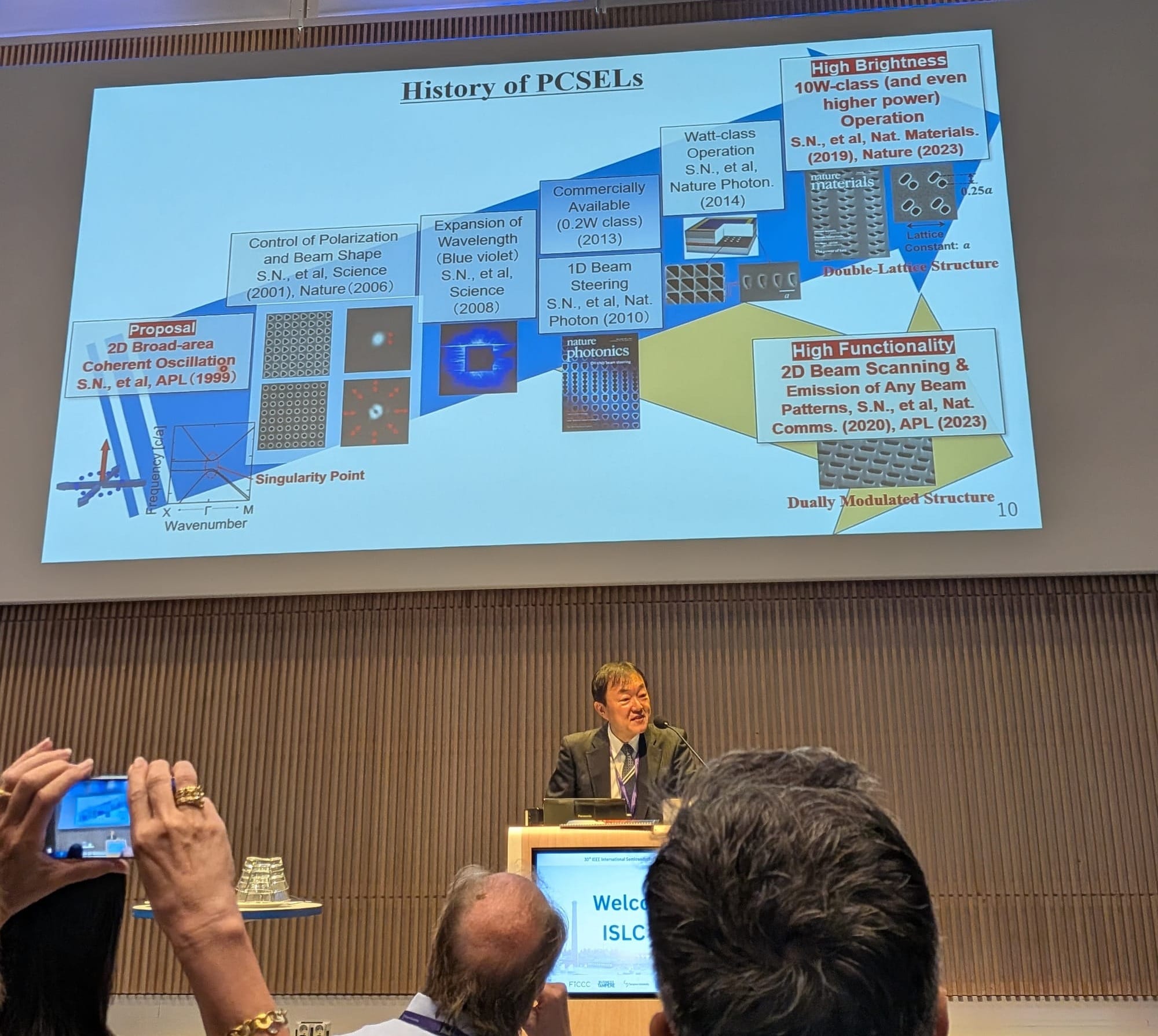
Noda's group broke that wall with the 2019 double-lattice photonic crystal (Yoshida, De Zoysa et al., Nature Materials 18, 121, 2019): two offset lattices that load obliquely-emitting higher-order modes with high radiative loss while the vertical fundamental stays low-loss. This is selective mode discrimination, not merely a bigger cavity, and the group formalized it via Hermitian / non-Hermitian coupling in 2022 (Inoue et al., Nature Communications 13, 3262). The 2023 flagship carried it to a device (Yoshida et al., Nature 618, 727, 2023): a 3 mm aperture at >50 W continuous-wave, single-mode, 0.05° divergence, 1 GW·cm⁻²·sr⁻¹, the highest published single-chip continuous-wave single-mode brightness to date.
On efficiency, multi-junction active layers give a 3 mm two-junction PCSEL a 1.58 W/A slope (0.73 W/A single-junction) and a 1.8 kW pulsed peak (Katsuno et al., Applied Physics Express, 2024), though that paper measured only current versus optical power, not voltage or wall-plug efficiency. Keep the regimes separate: 1 GW·cm⁻²·sr⁻¹ is the 2023 continuous-wave value; 1 cm / 500 W is pulsed and conference-only; 1 kW and >60% WPE remain projections. The contribution that matters is the loss-engineering that lets brightness scale by area rather than by power density, the difference between a chip that cooks and one that merely needs its heat removed.
Boundary: Building It in the Hardest Material System
Research group: Prof. Åsa Haglund's group, Chalmers University of Technology; UV epitaxy from TU Berlin / Ferdinand-Braun-Institut (Kneissl, Wernicke)
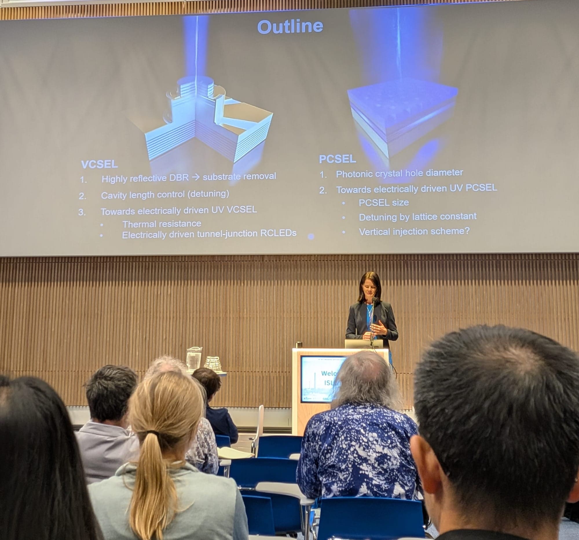
The PCSEL's difficulty shows most clearly in Haglund's ultraviolet work. This year her group reported the world's first deep-ultraviolet (UV-C, <280 nm) PCSEL (Apaydın et al., Laser & Photonics Reviews 20, e00271, 2026): single-mode, around 279 nm, <1° divergence, regrowth-free, and optically pumped. Be precise on that last point: watt-class output and electrical injection are stated in the paper as future goals, not results.
What the group owns is a process-and-integration toolbox: photo-assisted electrochemical etching for membrane release, dielectric DBRs, and tunnel junctions, carried across a string of firsts (the first UVB VCSEL, Hjort et al., ACS Photonics 8, 135, 2021; the first UVC VCSEL with <1% cavity-length control, Torres et al., Laser & Photonics Reviews 19, 2402203, 2025; and the deep-UV PCSEL above).
The hard part is realizing two-dimensional photonic-crystal coupling in the extremely low-index-contrast AlGaN/AlN system and in the deep ultraviolet, then using the hole fill factor (~15% works best) to select which band lases and so shape the far field. The lesson of this axis: the difficulty is not the design, it is making the device stable and precise. That capability is a learning curve measured in years, not a drawing.
Route: Making a High-Power PCSEL Manufacturable
Research group: Dr. Paul Crump's group, Ferdinand-Braun-Institut (FBH, Berlin); theory from the Weierstrass Institute (WIAS: Radziunas, Kuhn); process with the University of Glasgow (McKenzie)
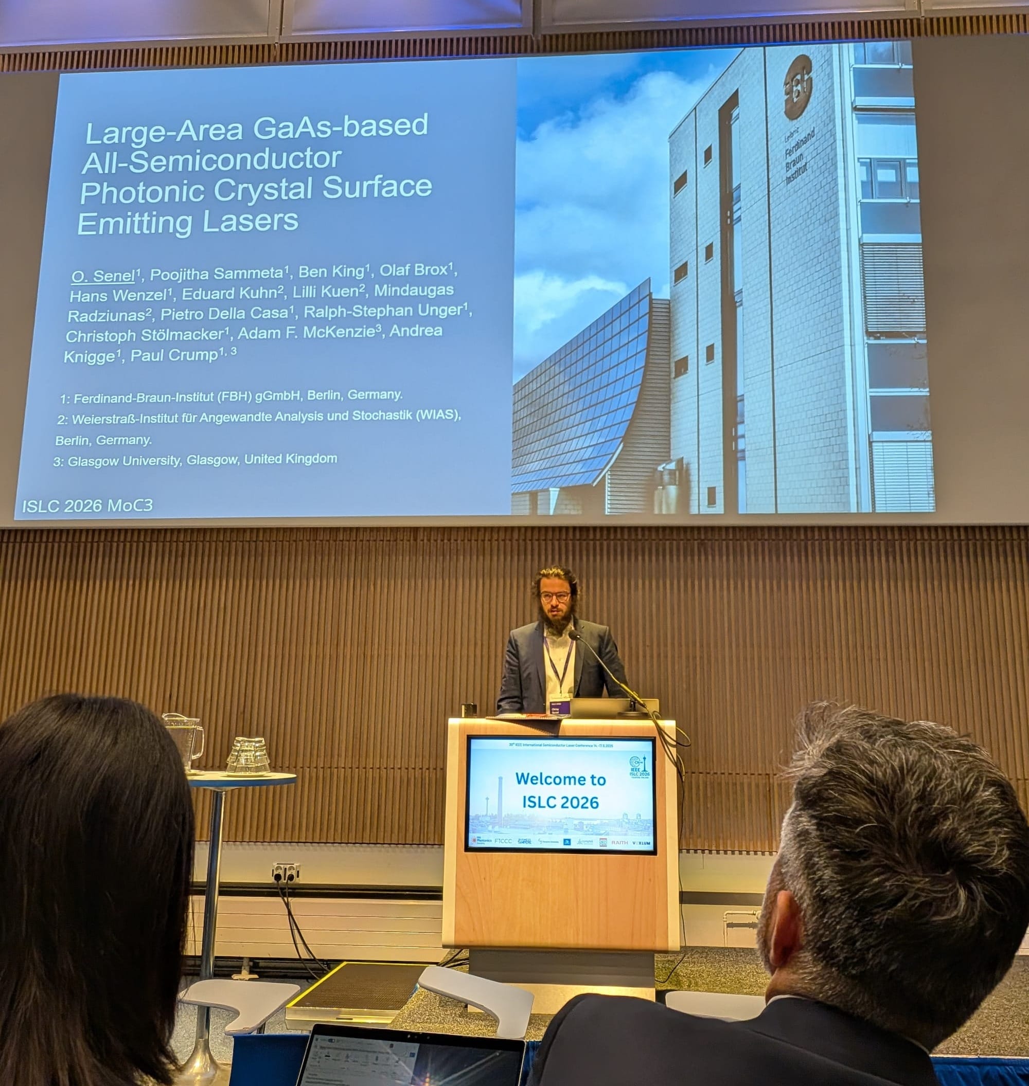
FBH plays a different role from the university labs: a high-power diode-laser institute trying to make the large-area PCSEL manufacturable, aimed at industrial and energy/defense pumping rather than the datacenter. Its design lever differs from Noda's: where Kyoto uses a double lattice, FBH and WIAS use a single-lattice "SIT" (stretched isosceles triangle) cell (King et al., Optics Express 32, 44945, 2024; Radziunas et al., Optics Letters 50, 1953, 2025), built by an all-semiconductor etch-and-regrow process (etch InGaP pillars, regrow GaAs by MOVPE; Sammeta et al., Micro and Nano Engineering, 2026), a different manufacturability path from Vector Photonics' no-regrowth single deep-air-hole etch.
State the status precisely: as of mid-2026 those core papers are design, simulation, or process, and no peer-reviewed paper reports a measured FBH PCSEL device. The device figures (>200 mW CW, >2.5 W pulsed, ~0.2 W/A slope, asymmetric far-field) appear only in the ISLC 2026 talk (O. Senel), a just-disclosed first-generation device, well below Noda in power and not yet symmetric in beam. This is an early, simulation-led program, not a product.
Its weight is institutional, not performance: one of Europe's leading high-power diode-laser houses, with the PCSEL riding its energy/defense pump franchise. Paul Crump co-chairs the diode working group of the DOE's LLNL-led IFE-STARFIRE fusion hub (2025) and co-authored a fusion-pump diode review with LLNL (Crump, Fenwick et al., Optics Express 33, 46456, 2025; about 2 kW/bar), alongside Germany's BMBF DioHELIOS (kW-class multi-junction bars, target <1 cent/W) and the in-situ monitoring project HOTSTACK. The point of this axis: the contest is also about who can manufacture a reliable, affordable high-power PCSEL, and it ties the technology to a market the others do not touch, fusion pumping and defense.
Market: A Commercialization Curve That Began in 2013
Commercialization is not new. Hamamatsu, with Kyoto, shipped a 0.2 W-class PCSEL in 2013, the first commercial one; a watt-class research demonstration (1.5 W CW) followed in 2014. The past few years have added a broad wave of productization across vendors, regions, and applications:
| Vendor / Institution | PCSEL direction | Progress (public information) |
|---|---|---|
| Hamamatsu Photonics (JP) | Earliest commercial PCSEL | 0.2 W-class commercial (2013); watt-class R&D demo (2014); long-standing Kyoto collaboration |
| Sumitomo Electric (JP) | InP 1.3 / 1.55 µm (telecom, FSO, sensing) | Double lattice: 200 mW (2022), metal-mirror 400 mW (2023), in-plane heterostructure 700 mW |
| Stanley Electric × Nichia × Kyoto (Noda) | Social implementation, blue/visible | Joint research from 2024; Φ1 mm highly directional beam |
| Mitsubishi Electric (JP) | High power, laser processing | Kyoto collaboration; ten-PCSEL two-row array module; commercialization planned 2026–27 |
| Rohm (JP) × Hokuyo × Kyoto | LiDAR | High-resolution PCSEL LiDAR demonstrated |
| Vector Photonics (UK, Glasgow spin-out) | Datacenter / co-packaged optics (CPO) | Uncooled 1 W, 1310 nm CW; real optical-comms transmission demonstrated |
| Huawei (UK, Ipswich Research Centre) | AI / datacenter interconnect | Multi-wavelength InP "quad-PCSEL"; conference-disclosure stage |
Two cautions when citing this: Huawei's multi-wavelength PCSEL is conference-disclosure-stage R&D (PCSEL Workshops, Aston 2024 and Glasgow 2025), not a product, and in datacenter/CPO Vector Photonics is further along while Kyoto holds the 1.3 µm InP telecom lineage. No single company is "the inflection." The real signal is breadth: AI interconnect, laser processing, LiDAR, free-space optics, and fusion pumping are pulling on one high-efficiency, wafer-scale light source at once.
Convergence: The Judgments
Across the four axes, the PCSEL is shifting from "will the physics work" to "who can turn it into a platform." Four judgments:
- Watch continuous-wave single-mode brightness, not peak watts. The published single-chip record is 50 W / 3 mm / 1 GW·cm⁻²·sr⁻¹ (Nature 2023); higher numbers are mostly pulsed or projected.
- The moat is process calibration and system integration, not the bare chip. Noda's loss engineering, Haglund's UV toolbox, and FBH's manufacturing backbone are hard to copy precisely because they are accumulated capability.
- It is a multi-market story. Datacom and AI interconnect, laser processing, LiDAR, and government-funded energy/defense pumping are pulling at once.
The PCSEL will not replace every laser tomorrow. But the curve since 2013 and the recent maturation of frontier, boundary, and route put it past "is this possible" and into execution, which is usually where the opportunity and the risk both live.